In modern PCB assembly, solder paste plays a critical role in creating reliable connections between electronic components and printed circuit boards. Even a small variation in solder paste volume, position, or coverage can lead to soldering defects later in the assembly process. Solder Paste Inspection (SPI) is used to detect these issues before components are placed and soldered.
SPI is an automated inspection method that evaluates solder paste deposits on a PCB after printing. By identifying problems early, manufacturers can correct the printing process before defective boards move further through production.
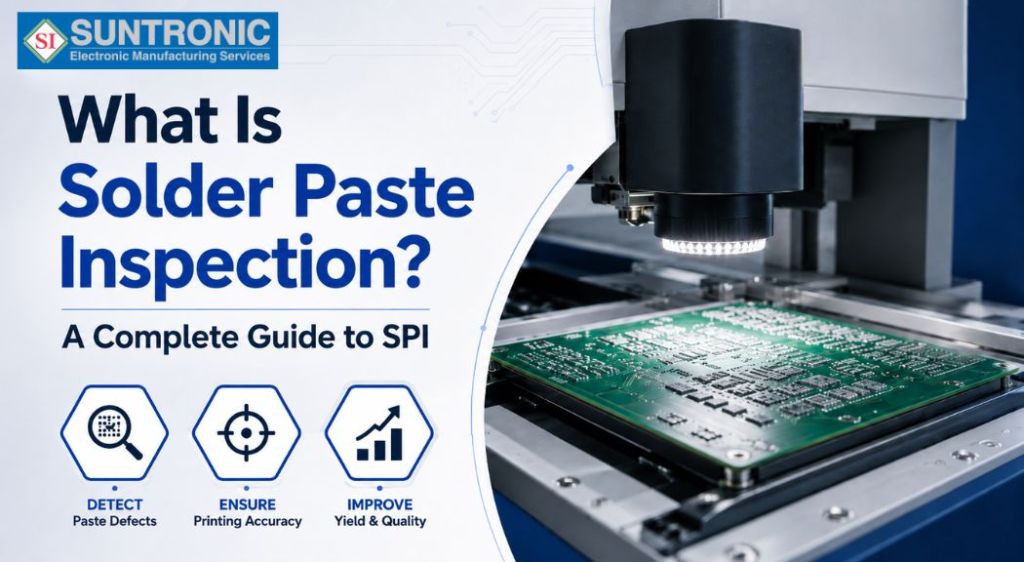
What is Solder Paste Inspection?
Solder Paste Inspection (SPI) is an automated process that checks whether solder paste has been applied correctly to PCB pads before component placement and reflow soldering. It measures important factors such as paste position, area, height and volume to identify printing problems that may affect the final assembly.
SPI helps solve common PCB assembly issues such as insufficient or excessive solder paste, paste misalignment, bridging and uneven deposits before they become costly soldering defects. By catching these problems early, manufacturers can reduce rework and scrap, improve solder joint quality and maintain consistent PCB assembly results.
Why is Solder Paste Inspection Important?
Solder paste printing is one of the earliest and most important stages of surface mount technology (SMT) assembly. A defect introduced during printing can remain hidden until after component placement or reflow soldering.
SPI helps manufacturers identify these problems at an early stage, when corrections are easier and less costly.
For example, if a stencil becomes clogged and deposits too little solder paste on several pads, SPI can identify the reduction in paste volume. The printer can then be adjusted or cleaned before more PCBs are processed.
SPI is important because it can help:
- Detect solder paste printing defects early
- Reduce rework and scrap
- Improve solder joint consistency
- Maintain accurate paste volume and placement
- Support stable SMT production
- Reduce the risk of defects after reflow
- Provide process data for quality control
For high-volume production, early defect detection can prevent the same printing problem from affecting hundreds or thousands of boards.
How Does Solder Paste Inspection Work?
An SPI machine examines solder paste deposits using optical imaging and three-dimensional measurement techniques. Modern systems commonly use 3D inspection to determine the height, area and volume of each deposit.
The process generally begins when a freshly printed PCB enters the SPI system. The machine captures detailed images of the solder paste deposits and compares the measured results with predefined inspection criteria.
If a deposit falls outside the acceptable limits, the system flags it for review. Depending on the production setup, the operator or process engineer can then investigate the printer, stencil, squeegee, solder paste, or PCB.
The inspection data can also reveal trends. For example, a gradual reduction in solder paste volume across multiple boards may indicate stencil contamination or changes in printing conditions.
Solder Paste Inspection Process: A Step-by-Step Guide
1. PCB Solder Paste Printing
Solder paste is applied to the PCB through a stencil. The stencil openings correspond to the pads where surface mount components will be placed.
2. PCB Enters the SPI System
After printing, the PCB is transferred to the SPI machine. Inspection takes place before component placement, allowing printing problems to be detected without disrupting later assembly stages.
3. Image and 3D Data Capture
The SPI system scans the board using cameras and optical measurement technology. It collects information about individual solder paste deposits.
4. Deposit Measurement
The system measures important characteristics such as paste volume, height, area and position. These measurements are compared with programmed acceptance limits.
5. Defect Identification
If the solder paste deposit is too small, too large, incorrectly positioned, or otherwise outside the defined limits, the system marks it as a potential defect.
6. Process Correction
The inspection results can help the production team identify the cause. Adjustments may include cleaning the stencil, changing printing parameters, checking paste condition, or correcting alignment.
7. Production Continues
Once the printing process is within the required specifications, the PCB proceeds to component placement and reflow soldering.
Types of Solder Paste Inspection Systems
SPI systems can differ based on their inspection technology and measurement capabilities. The two broad categories are 2D SPI and 3D SPI.
SPI Type | What It Measures | Main Advantage | Typical Limitation |
2D SPI | Paste presence, area and position | Fast and useful for basic inspection | Limited information about paste height and volume |
3D SPI | Paste height, volume, area and position | Provides detailed measurement of paste deposits | Generally more complex and costly than basic 2D inspection |
2D SPI primarily analyzes the appearance and coverage of solder paste from a two-dimensional image. It can identify missing deposits, misplaced paste and certain bridging conditions.
3D SPI adds height measurement, allowing the system to calculate solder paste volume. This provides a more detailed understanding of the printing process and is particularly valuable for fine-pitch and high-density PCB assemblies.
Benefits of Solder Paste Inspection in PCB Assembly
Early Defect Detection
SPI identifies solder paste problems before component placement and reflow. This makes it possible to correct the issue before it develops into a more difficult soldering defect.
Better Process Control
Inspection data provides measurable information about the printing process. Manufacturers can use this data to identify changes and maintain consistent production conditions.
Reduced Rework and Scrap
Finding printing defects early can reduce the number of boards that require repair after reflow. This can lower material waste and production costs.
Improved Solder Joint Reliability
Consistent solder paste deposition supports the formation of reliable solder joints during reflow. Correct paste volume and placement are especially important for components with small or closely spaced pads.
Support for Fine-Pitch Assembly
As component sizes become smaller and PCB designs become more compact, solder paste printing becomes increasingly precise. SPI helps verify that deposits meet the requirements of these demanding assemblies.
Data-Driven Manufacturing
Modern SPI systems can generate inspection data that helps production teams track trends, identify recurring problems and optimize the solder paste printing process.
Why Choose Suntronic for PCB Soldering?
Suntronic provides reliable PCB soldering services using advanced automated selective soldering equipment and precise process controls. Our capabilities support complex PCB assemblies, including mixed SMT and through-hole components, dense layouts, connectors and challenging soldering areas.
Our experienced engineering and production teams carefully control soldering temperature, flux application, solder volume, nozzle selection and soldering time to achieve consistent and reliable solder joints. We also use appropriate inspection and quality-control practices to identify process issues early and maintain production consistency.
From prototypes and low-volume production to higher-volume PCB assembly, Suntronic focuses on quality, precision and cost-effective manufacturing. Our integrated PCB assembly capabilities make us a dependable partner for reliable and consistent electronic manufacturing.
Conclusion
Solder Paste Inspection is an important quality-control step in modern PCB assembly. By measuring solder paste deposits before component placement, SPI helps manufacturers detect problems with volume, height, area and positioning at an early stage.
While 2D systems can provide useful visual inspection, 3D SPI offers more detailed information about solder paste volume and height. When combined with controlled printing parameters and effective process monitoring, SPI can help reduce defects, minimize rework and improve the consistency of SMT assembly.
For manufacturers working with fine-pitch components, complex PCB designs, or demanding production requirements, understanding and properly applying SPI can make a significant difference in overall assembly quality.

David Ly
David Ly is the Chief Operating Officer (COO) at Suntronic Incorporated, a prominent electronics manufacturing services (EMS) provider headquartered in Richardson, Texas. He leads the company's daily operations, strategic business objectives, and technology-driven product development.