Designing a printed circuit board is a deeply technical task that blends electrical engineering with practical manufacturing knowledge. While a schematic tells you how a circuit should function, the PCB layout determines how well that circuit performs in the real world. Many new designers focus on component connections but overlook critical PCB Layout Considerations, manufacturing constraints and environmental factors. As a result, early prototypes often fail due to noise, thermal issues, or poor routing.
Understanding What is PCB layout?, how PCB layout works and why PCB Layout Rules exist is essential for designing stable, reliable and cost-effective circuit boards. A good PCB Design Layout doesn’t just connect components it enhances signal quality, improves durability and ensures manufacturability.
This guide covers the complete foundation of PCB Layout Guidelines, essential design steps, routing practices, environmental considerations and the common mistakes beginners should avoid.
What Is PCB Layout and How It Works?
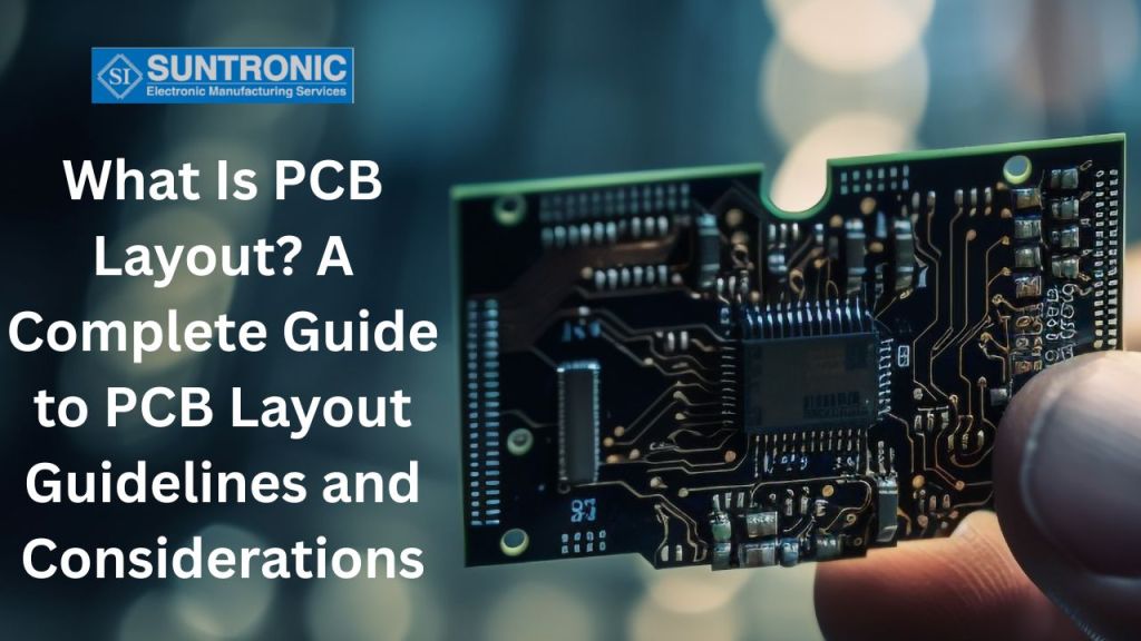
PCB layout is the process of arranging electronic components on a printed circuit board and connecting them through copper traces to create a functional circuit. After completing the schematic design, engineers translate it into a physical PCB design using specialized CAD tools.
How PCB Layout Works
The process begins with placing components logically, optimizing trace routing, defining copper areas and ensuring each signal path meets electronics and mechanical performance requirements. Various PCB Layout Considerations such as trace length, grounding strategy, thermal management and spacing ensure the board functions efficiently in real-world conditions.
Key PCB Layout Considerations Before Designing
Before starting PCB routing, designers must evaluate:
- Board size and component density
- Power distribution strategy
- Thermal Issues in PCB and heat dissipation needs
- EMI/EMC sensitivity
- Mechanical constraints and mounting requirements
These PCB Design Guidelines form the foundation of a successful layout.
Basic PCB Design Rules Every Beginner Must Follow
Whether you’re new to PCB design or revising your workflow, following Basic PCB Design Rules is essential to avoid functional issues or manufacturing defects. These rules ensure proper spacing, mechanical fit and electrical performance.
Essential Basic PCB Design Rules for Beginners
- Component Placement Rules
Start with connectors, power modules and high-current components. Keep sensitive analog parts away from noisy digital circuits. - Trace Width and Spacing Rules
Trace width must support the required current. Spacing must prevent arcing or signal interference. - Via Usage Guidelines
Vias should be minimized in high-speed routes. Use thermal vias to reduce overheating. - Grounding Rules
Solid ground planes improve signal integrity and reduce noise.
Key Basic PCB Design Principles
- Maintain consistent spacing between high-voltage and low-voltage traces
- Keep power traces thicker than signal traces
- Ensure return paths are short and direct
- Avoid placing components directly at board edges
By adhering to these PCB Design Rules, beginners avoid many Common PCB layout mistakes that often lead to redesigns or failures.
Step-by-Step PCB Layout Design Guide
Designing a printed circuit board requires careful planning and attention to detail. Following a structured approach ensures your PCB performs reliably and meets manufacturing standards. This Step-by-Step PCB Layout Design Guide outlines the essential pcb layout design steps while emphasizing important PCB Layout Considerations and PCB Design Layout Guidelines.
Step 1: Define Design Requirements
Before starting, list all electrical and mechanical requirements. Understanding the circuit functionality and limitations helps you follow proper PCB Design Guidelines and avoid costly errors later.
Step 2: Create a Schematic
A clear schematic is the foundation of any PCB. Ensure all connections are correct, as mistakes here can complicate later stages and violate PCB Design Rules.
Step 3: Component Placement
Place components logically to optimize signal flow. Follow PCB Layout Guidelines to minimize trace length and interference. Critical components like power supplies and high-speed ICs should be placed first.
Step 4: Routing and Trace Design
Route traces according to PCB Layout Rules. Maintain proper spacing, trace width, and layer usage as defined in Basic PCB Design Rules. Pay attention to power and ground planes to reduce noise and improve signal integrity.
Step 5: Design Rule Check (DRC)
Use PCB software tools to verify compliance with PCB Design Layout. Check spacing, clearances, and layer assignments to ensure manufacturability.
Step 6: Review and Optimization
Review the design for potential issues such as thermal hotspots or signal interference. Optimize trace paths and component placement following PCB Layout Considerations.
Step 7: Finalize Design for Manufacturing
Prepare Gerber files and documentation according to PCB Design Layout. Ensure all PCB Design Rules are met before sending the design for fabrication.
Following these pcb layout design steps ensures a reliable, high-quality PCB that meets both functional and manufacturing standards.
Essential PCB Layout Guidelines for Efficient Circuit Design
Once the basics are in place, designers can focus on optimizing routing, grounding and power distribution. These areas determine overall circuit efficiency and long-term performance.
Routing lies at the heart of all PCB Design Guidelines. Clean and direct routing improves signal integrity, reduces electromagnetic interference and simplifies debugging. Signals should follow the shortest and most predictable paths. High-speed and noise-sensitive signal traces must be kept separate from power lines or switching circuits. These PCB Layout Guidelines ensure stable communication and reduce crosstalk.
Grounding is equally critical. A well-designed ground plane stabilizes voltage references, filters noise and enhances return paths for high-frequency signals. Fragmented ground regions, on the other hand, cause unpredictable behavior. Designers should avoid unnecessary splits and preserve a continuous ground layer whenever possible.
Power distribution influences the electrical robustness of the design. Wide traces, proper decoupling capacitor placement and short return loops are essential. Understanding these PCB design best practices keeps voltage drop low and prevents unwanted oscillations.
Key PCB Layout Considerations for Reliable Board Performance
Reliability is a core goal of PCB design. To achieve this, engineers must evaluate multiple advanced PCB Layout Considerations, including thermal performance, high-speed behavior and manufacturability.
Thermal Issues in PCB
Heat buildup is one of the biggest threats to PCB durability. Poor thermal design leads to component failure, warping and reduced operational life.
Thermal management techniques:
- Add thermal vias under high-power devices.
- Use copper pours to spread heat.
- Keep heating components away from sensitive analog circuits.
- Use heat sinks or thermal pads where required.
EMI and Signal Integrity Considerations
Electromagnetic interference affects signal quality.
To reduce EMI:
- Maintain short return paths.
- Use ground planes strategically.
- Implement proper shielding and filtering.
High-Speed Design Considerations
As clock speeds increase, signal integrity becomes critical:
- Maintain controlled impedance.
- Follow differential pair routing rules.
- Avoid stubs or sudden layer transitions.
Mechanical Design Considerations
Mechanical integrity ensures safe PCB assembly and usage:
- Provide mounting hole clearances.
- Reinforce areas with connectors.
- Use keep-out zones near board edges.
These PCB Layout Considerations help design boards that perform reliably under real-world conditions.
PCB Design Rules and PCB Design Layout Guidelines for Better Manufacturability
A design is only successful if it can be manufactured consistently and cost-effectively. This is where Design for Manufacturability (DFM) becomes important. Following PCB Layout Rules for clearances, tolerances, drill sizes, pad size and copper spacing ensures smooth fabrication.
Many beginners focus solely on electrical behavior and overlook practical manufacturing limits. Each manufacturer follows standardized PCB Design Layout Guidelines and deviating from them often causes delays or failed boards. Ensuring correct annular rings, controlled impedance, minimal trace-to-edge spacing and realistic tolerances avoids redesigns.
Fabrication-friendly routing includes minimizing complex via structures, avoiding unsupported copper islands and keeping uniform copper distribution. Uneven copper leads to warping during the manufacturing process. These are core PCB design best practices that improve yield and reduce cost.
Even silkscreen placement matters text covering pads or vias leads to assembly defects. Designers must think of both the assembler and the fabricator while finalizing the PCB Design Layout.
Good manufacturability avoids prototype failures and accelerates the journey from idea to production.
Importance of PCB Layout Rules and Common PCB Layout Mistakes to Avoid
Adhering to PCB Layout Rules is essential for building reliable, high-performance printed circuit boards. These rules act as a framework that guides designers in creating layouts that are electrically stable, mechanically robust and easy to manufacture. Without following proper guidelines, even a well-designed schematic can lead to functional errors, manufacturing delays or long-term reliability issues once the product is deployed.
Why PCB Layout Rules Matter
PCB layout rules are designed to ensure that every element on the board from copper traces to components and vias works together efficiently. Following these rules offers several key benefits:
- Prevents short circuits and signal interference: Proper clearance, trace spacing and grounding protect the board from electrical failures and unwanted noise.
- Ensures thermal stability and a longer product lifecycle: Good thermal management practices help dissipate heat effectively, preventing component damage and performance drops.
- Improves manufacturability and reduces overall cost: A layout optimized for assembly and fabrication results in fewer errors, faster production and lower rework or testing costs.
- Supports industry safety and performance standards: Compliance with IPC and other standards ensures reliability across different environments and applications.
Common PCB Layout Mistakes to Avoid
Even experienced engineers can make errors that compromise board quality. Here are some frequent mistakes that should be carefully avoided:
- Poor component placement without logical flow, which complicates routing and increases signal path lengths.
- Incorrect trace width for high-current power lines, leading to overheating or voltage drops.
- Ignoring the return path for high-speed signals, causing EMI, noise and signal integrity issues.
- Placing vias too close to component pads, increasing the risk of solder bridging and manufacturing defects.
- Neglecting proper EMI shielding, resulting in interference and reduced device performance.
By understanding these risks and following established PCB layout guidelines, designers can achieve efficient routing, stable performance and a reliable final product.
Conclusion
Understanding What is PCB Layout? and applying proper PCB Layout Guidelines, PCB Layout Rules and PCB Layout Considerations is essential for producing robust electronic designs. Whether you’re focusing on routing, grounding, thermal behavior, EMI control or manufacturability, each step of the pcb layout design steps contributes to the final circuit quality.
Following Basic PCB Design Rules, avoiding Common PCB layout mistakes and adopting strong PCB design best practices ensures your board functions reliably under real-world conditions. As technology evolves, successful PCB designers must continually refine their knowledge, comply with updated standards and adapt their workflows to create efficient and manufacturable PCB designs.
If you consistently integrate these PCB Design Layout Guidelines into your process, you’ll produce high-quality, reliable and scalable PCB designs that stand the test of time.