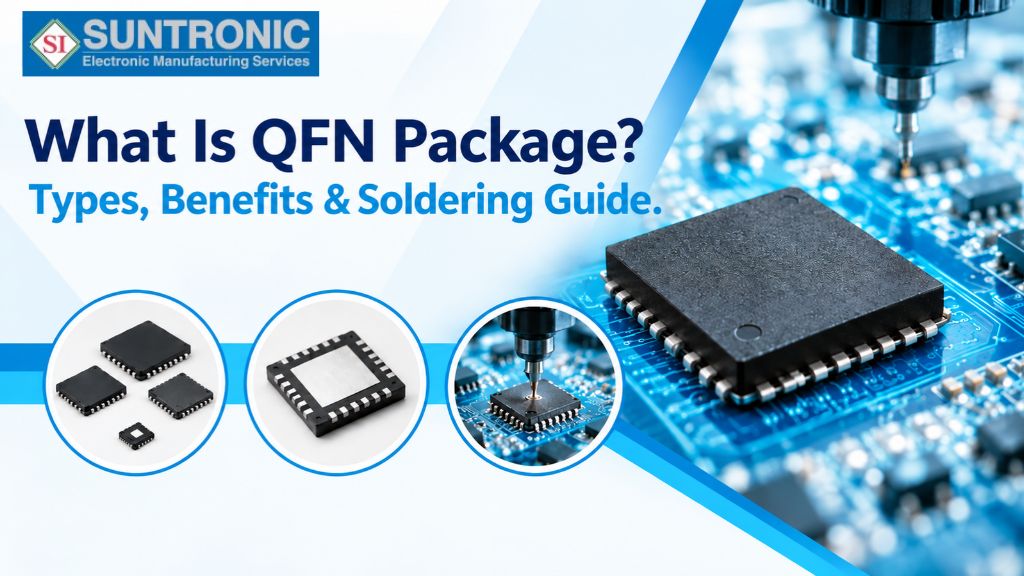
A QFN package (Quad Flat No-Lead) is a compact semiconductor package designed to save PCB space while providing efficient electrical and thermal performance. Unlike traditional packages with external leads, QFN components use terminals located underneath the package, along with an exposed thermal pad in many designs.
Because of their small footprint, low parasitic characteristics, and compatibility with automated SMT production, qfn packages are widely used in modern electronic devices. This guide explains what a QFN package is, its types, benefits, applications, soldering process, common problems, and how it compares with QFP.
What Is a QFN Package?
QFN stands for Quad Flat No-Lead. It is a surface-mount semiconductor package with a flat, rectangular or square body and electrical terminals positioned along the underside edges rather than extending outward as visible leads.
A typical qfn package may also include a large exposed thermal pad on its bottom surface. This pad can be soldered directly to a corresponding copper area on the PCB to help transfer heat away from the component.
Key Features of QFN Packaging
- Leadless construction: Electrical connections are located underneath the package.
- Compact footprint: QFN designs require less board space than many leaded packages.
- Exposed thermal pad: Many QFN packages provide a thermal path to the PCB.
- Low parasitic effects: Short electrical connections can help reduce inductance and capacitance.
- SMT compatibility: QFN components can be assembled using automated surface-mount equipment.
The combination of small size and efficient electrical and thermal characteristics makes qfn packaging suitable for space-constrained electronic products.
What Are the Types of QFN Packages?
QFN packages are available in different configurations to meet specific electrical, mechanical, thermal, and application requirements. Variations can be classified by package dimensions, terminal arrangement, and thermal-pad configuration.
Common QFN Variations
Standard QFN: A conventional QFN configuration used across many electronic applications.
Dual-Row QFN (DR-QFN): Uses two rows of terminals to provide a higher number of connections within a relatively compact footprint.
Micro QFN: Designed for applications where extremely small component dimensions are important.
Power QFN: Optimized for applications requiring improved thermal management and current-handling capabilities.
The appropriate package depends on factors such as available PCB area, number of required connections, operating temperature, electrical requirements, and thermal design.
What Are the Benefits of QFN Packages?
The growing use of QFN components is largely driven by the need for smaller and more efficient electronic products.
Compact Size and High PCB Density
Because QFN packages do not have leads extending beyond the package body, they can occupy less PCB area. This allows designers to place more components within a limited board footprint.
Low Parasitic Effects
The short connection path between the semiconductor die and PCB can help reduce unwanted parasitic inductance and capacitance. This can be particularly useful in high-frequency and high-speed electronic designs.
Good Thermal Performance
Many QFN packages include an exposed thermal pad that connects to a copper area on the PCB. When properly designed and soldered, this arrangement can provide an efficient path for heat transfer.
Automated Assembly
QFN components are suitable for automated SMT production, allowing manufacturers to integrate them into high-volume PCB assembly processes.
Where Are QFN Packages Used?
The compact form factor and electrical and thermal characteristics of QFN devices make them suitable for numerous industries and applications.
Common applications include:
Industry | Typical QFN Applications |
Consumer Electronics | Smartphones, wearables, audio devices, portable electronics |
Automotive | Control modules, sensors, power and communication systems |
IoT | Wireless modules, sensors, connected devices |
Industrial | Controllers, monitoring equipment, automation systems |
Medical Electronics | Portable and compact electronic devices |
Power Management | Voltage regulators, converters, drivers, and power ICs |
The specific application depends on the electrical specifications and package characteristics of the individual semiconductor device.
How to Solder a QFN Package?
QFN package soldering requires careful control because the terminals are located underneath the component and cannot be visually inspected as easily as traditional leads.
Step 1: Prepare the PCB
Ensure that the PCB footprint matches the manufacturer’s recommended land pattern. The solder pads should be clean and correctly sized.
Step 2: Apply Solder Paste
Use a stencil to apply solder paste accurately to the perimeter pads and exposed thermal pad. The paste volume should be controlled to minimize the risk of solder bridges and excessive voiding.
Step 3: Place the Component
An automated pick-and-place machine can position the QFN accurately over the PCB footprint. Proper alignment is important because the terminals are underneath the package.
Step 4: Reflow Soldering
The assembled PCB passes through a controlled reflow profile. The solder paste melts and forms electrical and mechanical connections between the QFN and PCB.
Step 5: Cooling
After reflow, the board should cool under controlled conditions to allow solder joints to solidify properly.
Step 6: Inspect the Assembly
Inspection may include optical inspection, X-ray inspection, and electrical testing. X-ray inspection is particularly useful for evaluating hidden solder joints and the exposed thermal-pad connection.
What Are Common QFN Soldering Problems?
Several issues can affect QFN assembly if the PCB footprint, stencil design, paste volume, placement, or reflow profile is not properly controlled.
Common problems include:
- Solder bridges: Excess solder can connect adjacent terminals.
- Insufficient solder: Too little solder may result in weak or open connections.
- Component misalignment: Incorrect placement can prevent proper pad-to-terminal contact.
- Thermal-pad voids: Entrapped gases can create voids underneath the exposed pad.
- Poor wetting: Incorrect process conditions can prevent proper solder bonding.
- Open connections: Hidden terminals make some defects difficult to identify through visual inspection alone.
Using an appropriate stencil design, controlled solder-paste volume, accurate placement, optimized reflow parameters, and suitable inspection methods can help reduce these risks.
QFN vs QFP: Key Differences
Although both QFN and QFP are surface-mount packages, their physical construction and assembly characteristics differ.
Feature | QFN | QFP |
Leads | No external leads | External leads on four sides |
Package Size | Generally compact | Generally larger for equivalent connection requirements |
Thermal Pad | Often included | Typically uses different thermal-management arrangements |
PCB Space | Efficient for high-density layouts | Requires space for extending leads |
Inspection | Hidden connections can require X-ray | Leads are generally visible for optical inspection |
Assembly | SMT/reflow compatible | SMT/reflow compatible |
QFN is particularly useful when board space and thermal performance are important, while QFP can provide easier visual access to its external leads during inspection.
Why Choose Suntronic for QFN PCB Assembly?
Successful qfn package soldering depends on more than simply placing a component on a PCB. Accurate component placement, solder-paste control, reflow optimization, inspection, and testing all contribute to assembly quality.
Suntronic provides QFN and SMT PCB assembly solutions supported by precision manufacturing processes and quality-focused production practices. Its electronics manufacturing capabilities can support different PCB assembly requirements, from component placement and soldering through inspection and testing.
For projects involving compact, high-density PCB designs, working with an experienced electronics manufacturing partner can help address the specific assembly requirements associated with QFN components.
Need reliable QFN PCB assembly for your compact, high-density electronic designs? Contact Suntronic today to discuss your QFN and SMT PCB assembly requirements.

David Ly
David Ly is the Chief Operating Officer (COO) at Suntronic Incorporated, a prominent electronics manufacturing services (EMS) provider headquartered in Richardson, Texas. He leads the company's daily operations, strategic business objectives, and technology-driven product development.